 Fraunhofer USA Center Midwest CMW
Our research focuses on combining plasma science with materials processing to facilitate the exploration of advanced functional coatings, next generation electro-optical devices, and energy storage devices. High-density plasma source science and engineering. Plasma sources are vitally important for manufacturing functional coatings, flat panel displays, solar cells, semiconductor integrated circuits, and optical thin films. Our research combines advanced modeling with innovative designs to develop high-performance plasma sources, such as inductively coupled high-density plasmas, ion sources, sputtering magnetrons, and magnetically enhanced plasmas. Plasma-assisted materials processing. The highly reactive species in plasmas enable efficient processing of advanced nanomaterials and surface engineering. We are particularly interested in understanding the gas-phase reactions and plasma-surface interactions. We use optical emission spectroscopy and probes to diagnose the reactions and plasma properties. Using a variety of plasma sources, we have been conducting research in diamond and diamond-like carbon coatings, piezoelectric thin films, transparent conductive oxide films, optical bio-sensors, and photovoltaic thin films and devices. We are also exploring plasma-assisted manufacturing of nanomaterials under the support of NSF. Our research on electro-optical thin films and optical filters includes extensive modeling using the state-of-the-art optical software. Nanostructured materials for energy storage and harvesting. We focus on nanoporous materials with large active surface areas for energy storage devices. We are particularly interested in using advanced plasma sources to modulate the electric properties of carbon nanomaterials. We also have active research in the electro-optical properties of porous silicon fabricated using non-HF solutions.
Plasma Sources and Processing
Modeling Plasma Discharges
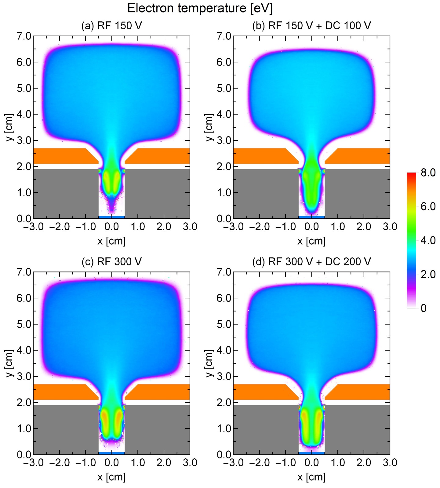
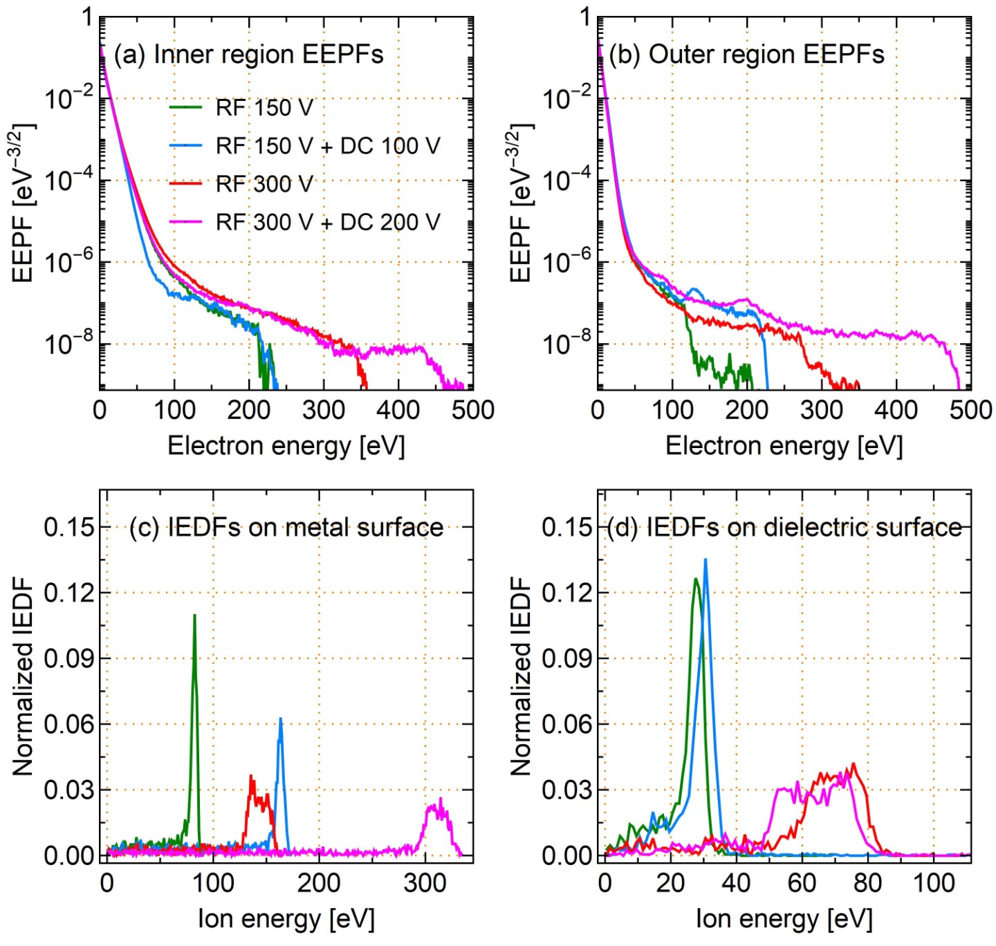
Radio frequency (RF) magnetron sputtering is an essential technology for manufacturing a broad variety of high-quality dielectric thin films. The ceramic targets, the source of the thin film coating material, consumed during the RF sputtering process are expensive, thus efficient target consumption is highly desirable in lowering manufacturing costs. Current magnetrons are designed for achieving optimum performance in direct current (DC) sputtering, which is used for target materials that are electrically conducting like metals. When this same magnetron is used for RF sputtering of insulator targets, it is ineffective and produces an abnormal erosion profile completely different from that in DC sputtering (see the figure below). Specifically, the intensively etched region under DC sputtering is the least eroded under RF sputtering. Incomplete understanding of the ceramic target etching mechanisms occurring during RF magnetron sputtering results in poor target use rates (~30%).This project aims to understand the mechanisms of the abnormal RF target erosion and fill the knowledge gap through 1) modeling RF magnetron discharges, and 2) developing highly efficient RF magnetrons. Our research has led to novel magnetrons with two times higher use rates of target materials. This will have a positive impact on many industrial fields including large-area optical coatings, energy storage, displays, solar energy, and semiconductor devices.
Our group can design circular RF sputtering magnetrons of 2"-8" diameters and rectangular magnetrons of any length.
Plasma Sources
We combine plasma modeling with experimental diagnostics to develop a variety of plasma sources to enhance the efficiency of materials processing. Applications include materials synthesis, low-temperature sterilization, and plasma etching. A few plasma sources we developed include single-beam ion sources (middle figure below), large-area rectangular sputtering magnetrons with high target use rates (right figure below), and inductively coupled plasma sources (left animation below, showing the evolution of plasma electron density in a magnetically enhanced inductive discharge).
Our group can help industry and research labs to design highly efficient DC sputtering magnetrons and ion sources.
Plasma Enhanced Materials Processing
Plasma Activation of Biochar
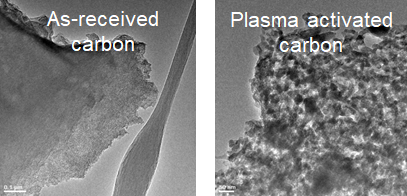
Biochar is a porous carbon material derived from biomass pyrolysis (Fig. 1). The porous structure leads to large surface areas attractive for advanced applications, including water treatment, energy storage, and air purification. Biochar must be activated to create nanostructures and promote the surface energy (making the surface active). The performance of biochar can be improved more than two-fold after activation; over 99% of toxic elements in polluted water can be trapped in activated biochar after a single pass.
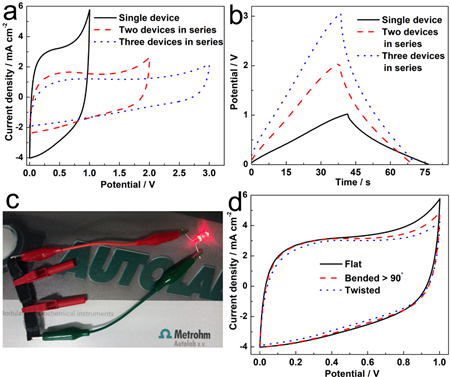
Conventional activation requires high-temperature chemical treatment (>900°C) for over two hours followed by washing and prolonged drying. This energy-intensive and lengthy treatment has been a critical barrier to commercializing biochar in advanced applications. Our group has developed a patented highly efficient plasma activation of biochar, which shortens the activation to less than 10 minutes without external heating. Figures below demonstrate the effects of plasma activativation on the performance of supercapacitors.
Energy Storage Materials and Devices
Our group has demonstrated an efficient radio frequency (RF) dielectric barrier discharge plasma for exfoliating of graphite oxide (GO) into graphene. The exfoliation occurred swiftly once the RF power and gas pressure reached a level that enabled sufficient energy transfer from the plasma to the GO. X-ray diffraction (XRD) and transmission electron microscopy (TEM) confirmed that graphene or carbon nanosheets were successfully prepared. The plasma exfoliation mechanism was revealed based on the microstructure characterization and optical emission spectroscopy, which indicated that oxygen was released at the moment of exfoliation. Supercapacitors fabricated using the plasma exfoliated graphene exhibited an initial specific capacitance of ~312 F g−1 under 0.1 A g−1charge/discharge current and ~100% retention after 1000 consecutive cycles under currents ranging from 0.1 to 10.0 A g−1 in 6 mol L−1 KOH electrolyte.
Nanostructured Materials
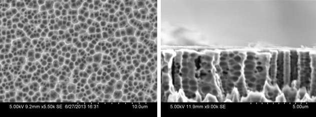
Our group has been working on developing porous silicon and porous carbon nanomaterials for energy storage, energy harvesting, and optoelectronic devices. The challenge is to understand the chemical and physical reactions that co-exist during the growth of nanoporous structures. We use advanced modeling to predict the plasma properties and guide experiment studies. We have successfully prepared 3D porous Si using non-HF solutions. The porous Si leads to significantly enhanced light trapping.