Diamond Electronics

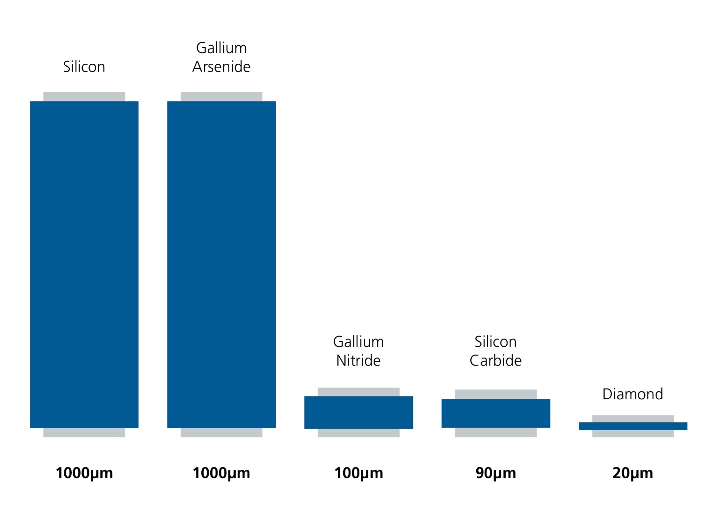
Diamond, among others, has properties which make it particularly useful as electronic material. As displayed by the figure of merit (Figure 1) it can be seen that key properties, such as the bandgap, the saturated electron drift velocity and the electric breakdown field outshine silicon by leagues, but also outperform current choices for high-power and high-frequency electronics, namely silicon carbide and gallium nitride (Figure 2). This makes diamond electronics particularly interesting for high-power and high-frequency applications. 

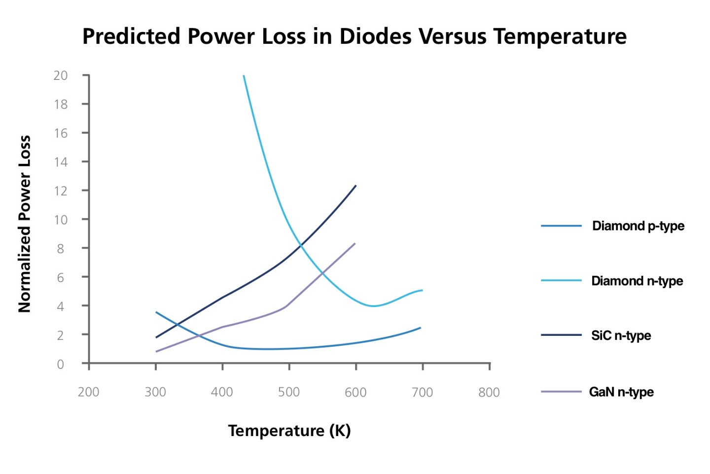
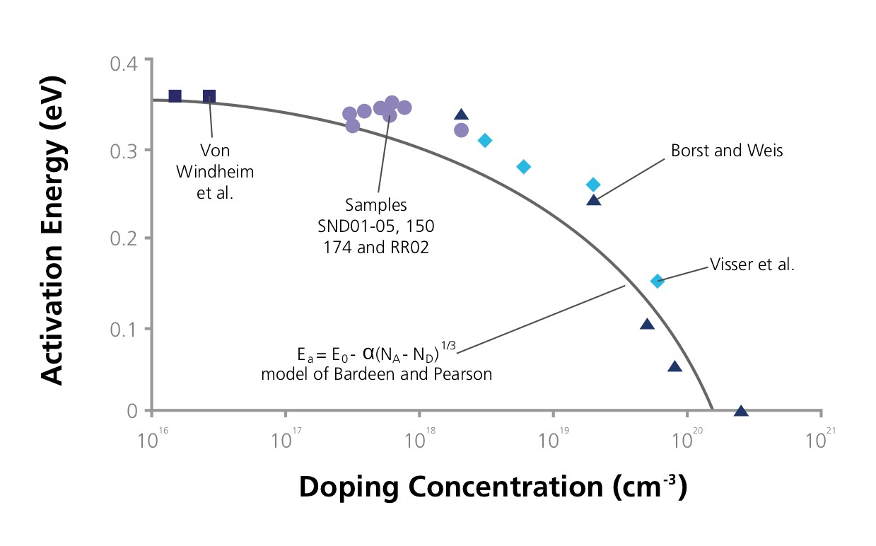
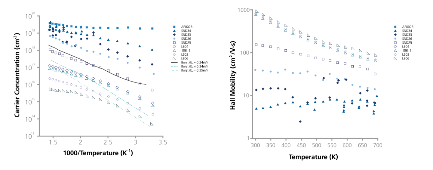
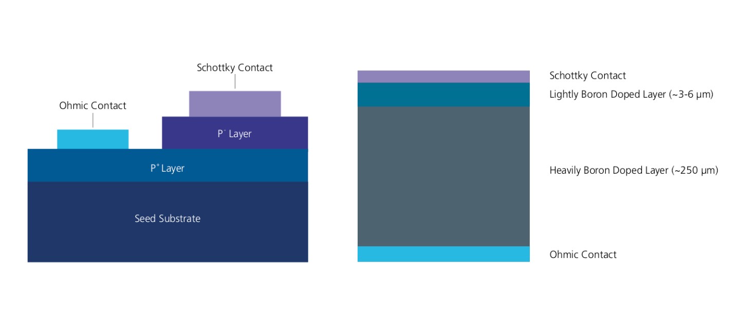
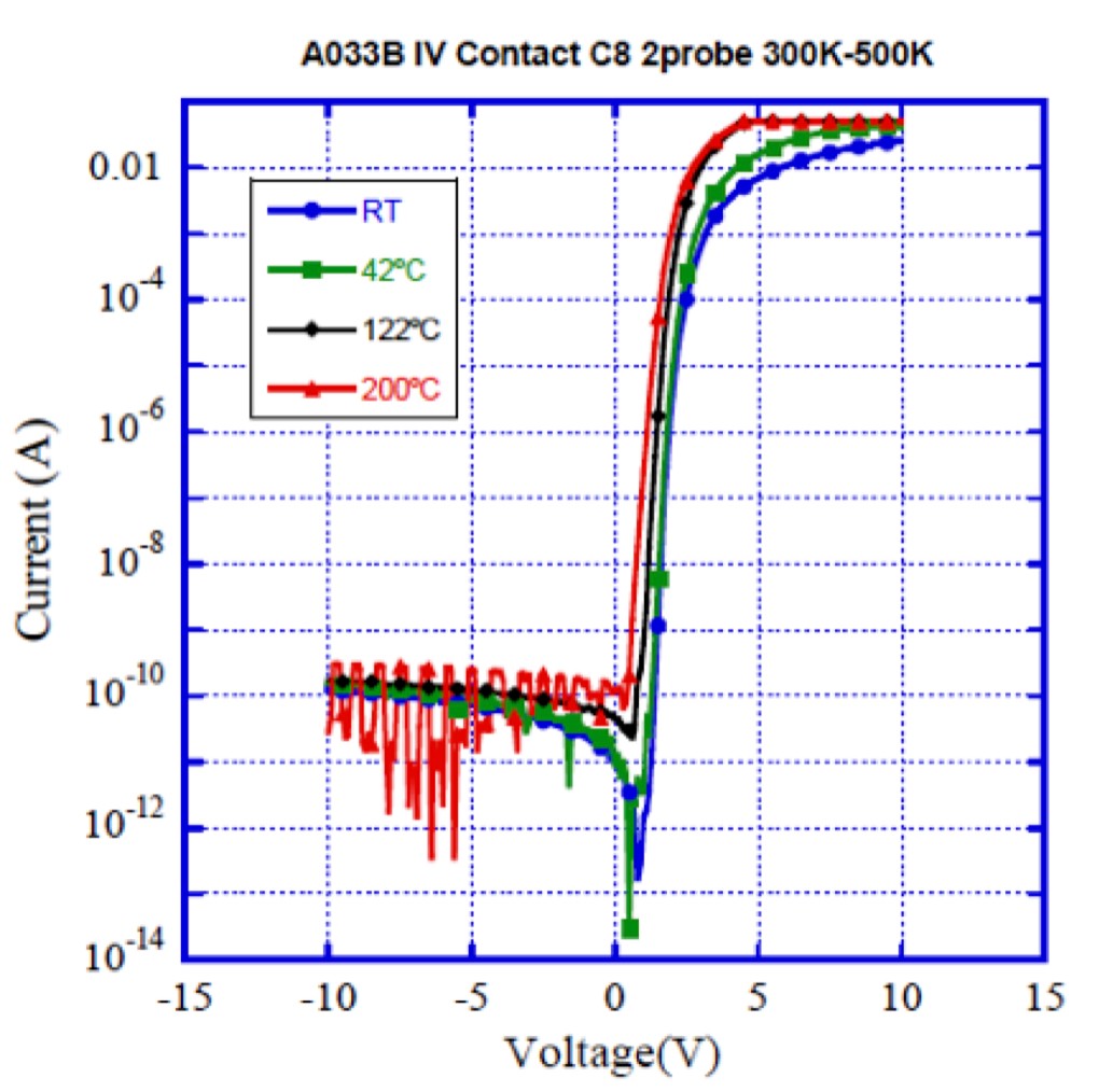
Conduction in diamond can be achieved by doping using boron for p-type conduction and phosphorus for n-type conduction. Both, p-type (0.37 eV) and n-type (0.55 eV) dopants are rather deep donors. This means that diamond electronics is actually performing best at elevated temperatures. This is in stark contrast to competing semiconductor materials such as SiC and GaN (Figure 3). With diamond’s performance being optimal above 300°C

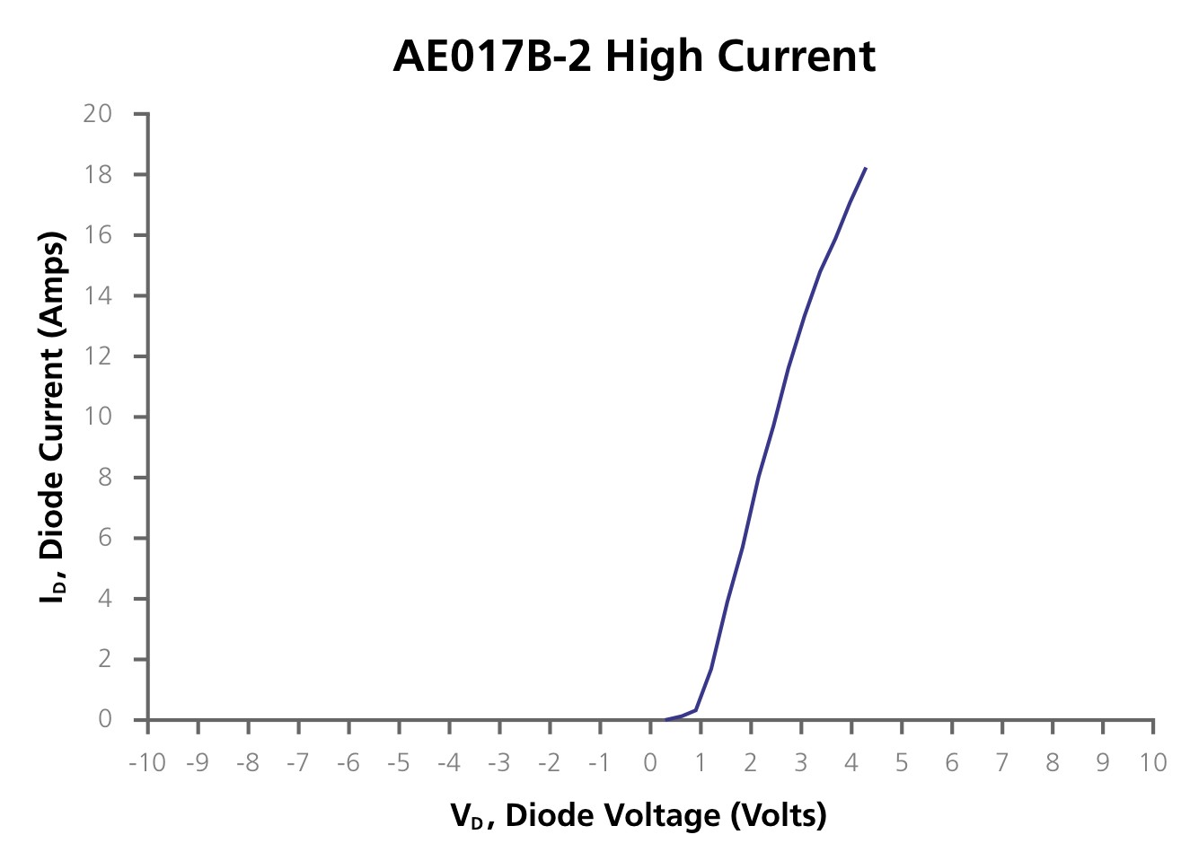
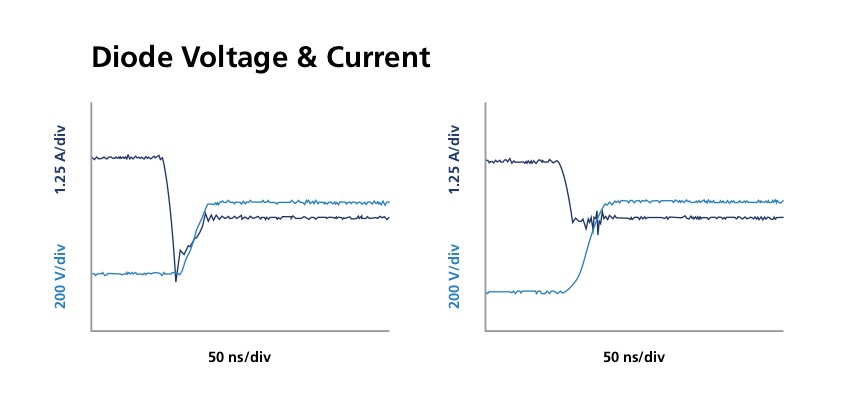
Diamond-based power electronics will operate safely at high temperatures without the extensive cooling and circuit protection required in today’s high-power systems. The exceptional semiconductor properties of diamond will enable a new class of high-power, high-voltage electronic devices and will transform applications in transportation, manufacturing, communication and energy sectors.

Figure 1
© Fraunhofer USA CMW
Figure 1 - Figure of Merit comparing properties of diamond to other semiconducting materials. All values have been scaled based on the base of the value of silicon being one
© Fraunhofer USA CMW
Figure 2 - Comparison of different semiconductor material vertical diodes designed to withstand an electric field of 10,000V
© Fraunhofer USA CMW
Figure 3 - Forward current power loss in high voltage diodes constructed from various semiconductors. The diodes are all designed to flow the same current and block the same high reverse bias voltage

P-Type Diamond Films

The incorporation of boron into diamond is rather common. This is causing a blue coloration, which makes the Hope diamond famous for. The blue coloration is caused by absorption effects due to the addition of the electron acceptor boron into the diamond lattice. At high enough concentrations near the semiconductor-metal transition, the film becomes solidly black and the bandgap drops to nearly 0 eV (Figure 4). 


Our facility has the capability to grow boron doped diamond films with incorporation levels ranging from 1014 (~570ppt) to 1021 (~0.6%) atoms/cm3. We offer the growth of a broad range of boron doped films in the lowly doped range (1015 to 1017) as well as heavily doped films (1018 to 1021) based on customer specifications. Sheet resistance of heavily doped films are usually below 10-2 Ωcm. Those films show a strong increase of conductivity and mobility with temperature (Figure 5). The doping concentration remains constant throughout the grown thickness 

© Fraunhofer USA CMW
Figure 3 - Boron-doped diamond
© Fraunhofer USA CMW
Figure 4 - Activation energies shown as reported in literature and model of Bardeen and Pearson
© Fraunhofer USA CMW
Figure 5 - Temperature dependent hall mobility of boron doped SCD at different doping concentrations

N-Type Doping

© Fraunhofer USA CMW
Figure 5 - N-Type diamond

Our center possesses the capability to grow n-type conducting diamond using phosphorus as a dopant. The obvious choice of nitrogen is non-practical due to its very deep donor level (1.7 eV). The donor level of phosphorus is still rather deep being 0.55 eV, which explains why the electric performance curve is shifted towards even higher temperatures compared to boron doped diamond (0.37 eV) (Figure 3).

We offer growth of phosphorus doped epilayers on insulating diamond substrates. This involves the growth of (111) oriented phosphorus films on (111) oriented seed substrates with phosphorus concentrations ranging from 1016 atoms/cm3 up to exceeding 1020 atoms/cm3. Additionally, we are able to grow (100) oriented n-type material on (100) seed substrates with phosphorus concentrations up to 1018 atoms/cm3.  

Finally, we offer selective growth of (111) areas on (100) seeds by using a patented substrate pre-treatment method. 

High Power Schottky Diodes

© Fraunhofer USA CMW
Figure 6 - Schematics of a pseudo-vertical (left) and a vertical (right) SBD design
© Fraunhofer USA CMW
Figure 7 - Forward current behavior of a vertical design SBD

A Schottky barrier diode (SBD) is a common semiconductor device for switching applications. It allows current conduction in its forward direction with a forward voltage applied, while also blocking significant reverse voltages.

Diamond based SBDs utilize a heavily boron doped layer for the current conduction, while a lowly boron doped layer provides the desired voltage breakdown strength. Different design realizations have specific advantages and disadvantages (Figure 6). Vertical diode designs result in superior current conduction behaviors but at the cost of lower breakdown strength. Vice versa, pseudo-vertical designs (Mesa) can withstand higher reverse voltages at the cost of a lower overall current rating.  

We demonstrated diode operation with forward currents exceeding 18 A (Figure 7) and withstanding reverse voltages beyond 1700 V (Figure 8). Overall, diode characteristics (IV curve) was achieved with a forward voltage drop below 1V (Figure 9). Switching times in the ns range have been achieved using boron doped diamond SBDs outperforming SiC without detecting parasitic capacitances (Figure 10).

Diamond based SBD main uses will be in reverse current discharge protection and as rectifier in power applications, i.e. switched-mode power supplies.

© Fraunhofer USA CMW
Figure 8 - Reverse voltage behavior of a mesa SBD using different Schottky metal contacts
© Fraunhofer USA CMW
Figure 9 - IV characteristics of a diamond SBD
© Fraunhofer USA CMW
Figure 10 - Comparison of the switching behavior of a SiC (left) and diamond (right) SBD

Field Effect Transistors

© Fraunhofer USA CMW
Figure 11 - Cross section of a p-type diamond FET using a lightly boron doped layer (p+) as conductive channel

Transistors are another common semiconductor device used to amplify or switch electrical power and are either bipolar junction transistors (BJT) or field effect transistors (FET). A transistor consists of three terminals (emitter(BJT)/drain(FET), collector(BJT)/source(FET) and gate) (Figure 11) while a SBD is a two terminal device (analogous to emitter and collector). In a transistor, current is flowing from source to drain while the gate is used to regulate the amount of current flow. The applied signal at the base is significantly smaller than at the other two terminals. Hence, a much larger signal is controlled with a significantly smaller signal making transistors efficient switches and amplifiers (large ratio of VC to VB).

Modern transistor realizations in diamond are usually FETs rather than JFETs, which are unipolar devices. Conduction is achieved either by hole conduction in a boron doped film (metal semiconductor FET – MESFET) (Figure 11) or through hole gas conduction of a hydrogen terminated diamond surface encapsulated by an oxide (metal oxide semiconductor FET – MOSFET). Transistor designs can be optimized for high-power or high-frequency applications.

Summary

We offer our expertise in the growth of doped epilayers (p-type and n-type) based on customer specifications regarding doping concentration and thickness. Beyond typical electrical characterization (IV, CV) we offer sophisticated testing capabilities such as temperature dependent Hall effect measurements.

Our team has extensive knowledge on device fabrication. We offer our expertise in consultation of designs for diamond electronics (Schottky diodes, P-N and P-I-N diodes, & FETs) based on your voltage, current and power needs. If desired, we can carry out the device fabrication, device packaging and testing in our facilities.

Please submit an inquiry for more in-depth information.