Boron-Doped Diamond Solutions

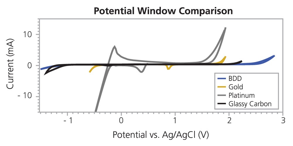
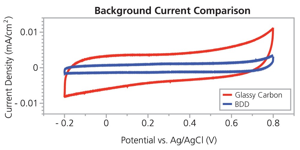
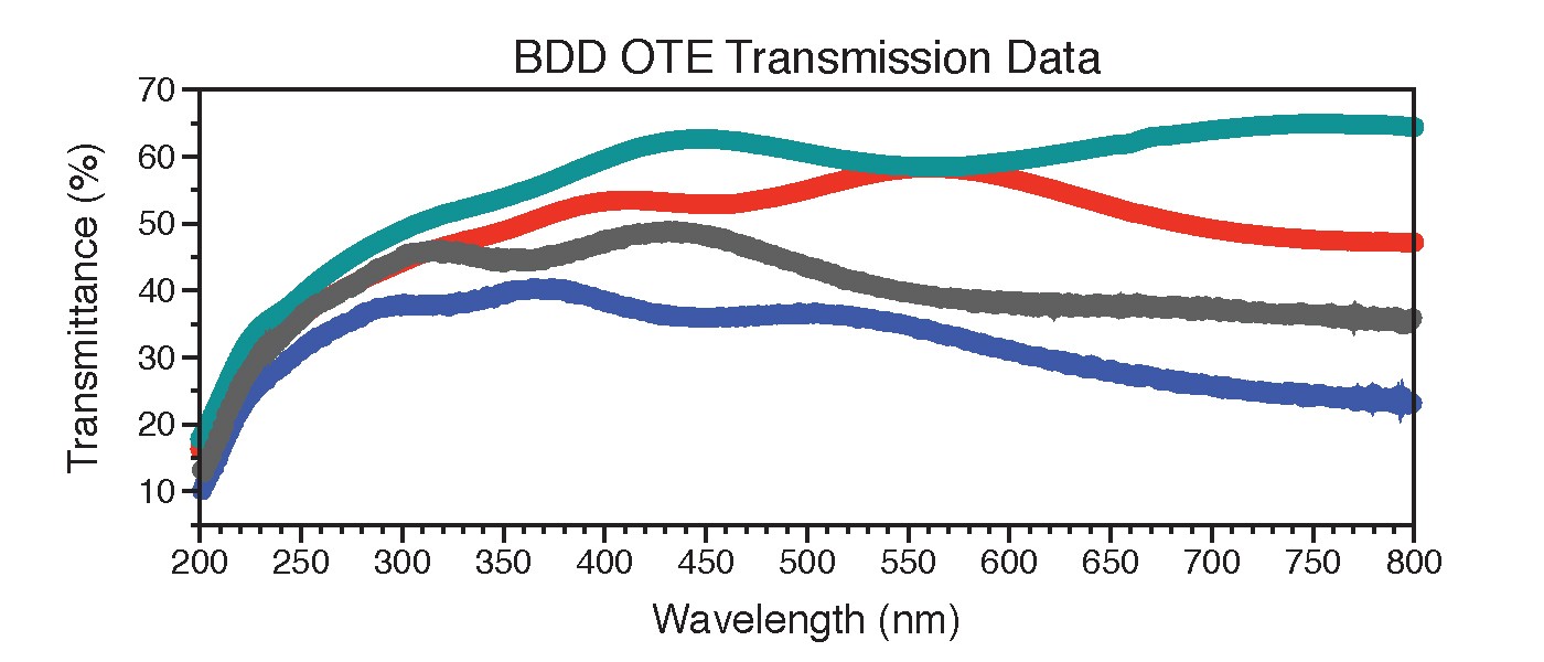
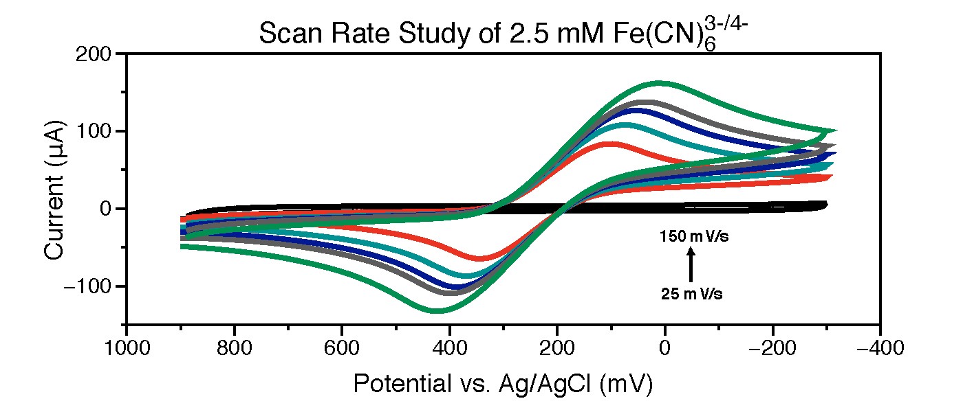
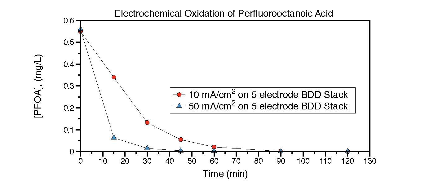
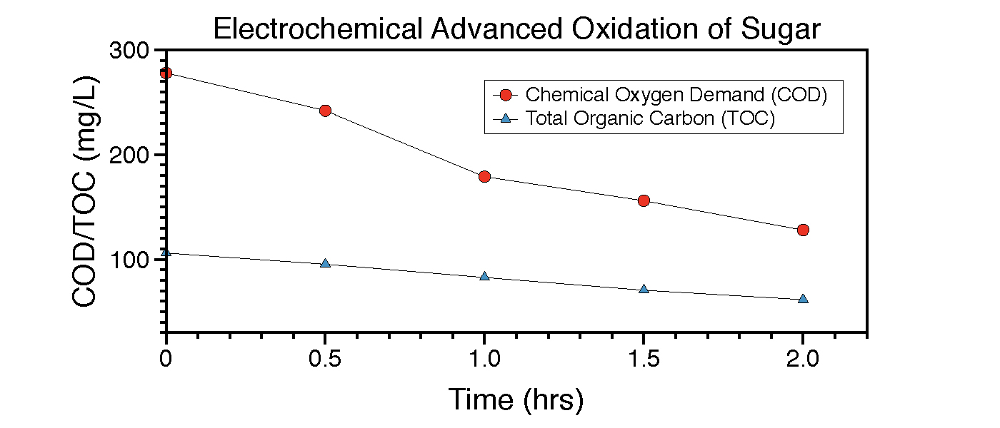
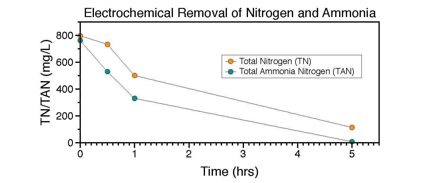
Boron-doped diamond (BDD) is an excellent electrode material with a large potential window in aqueous solution and low background current. The wider potential window and lower background currents make the BDD material very attractive for electrochemical analysis experiments. Reactions occurring in potential ranges from about -0.5V to -1.2V and about +1.8V to 2.5V can now be analyzed which could not be analyzed on traditional electrode surfaces such as Au and Pt. The lower background current allows for higher sensitivity and lower detection limits. Extreme stability, biocompatibility and resistance to surface fouling are added benefits to this exceptional electrode material.

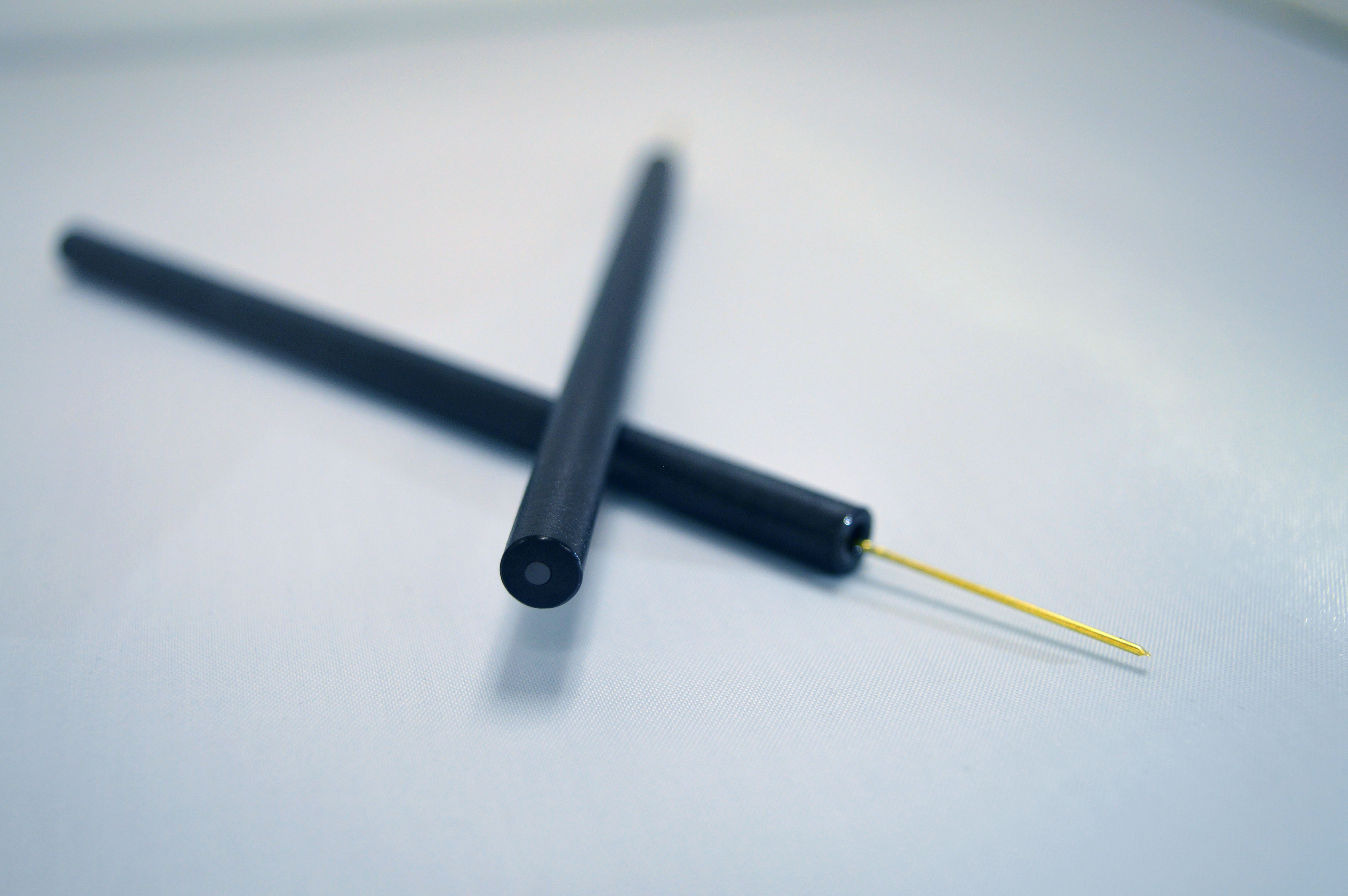
The Fraunhofer USA Center Midwest has developed a large portfolio of boron-doped diamond electrodes and materials targeting a broad range of markets including biotechnology, environment and health. The available portfolio is offered to collaborators and project partners to further advance the technology and develop products. The portfolio includes:

•          Thin film electrodes on silicon, quartz and metal substrates

•          Microfabricated 3-in-1 electrodes and micro electrode arrays

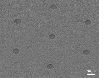
•          Optical transparent electrodes

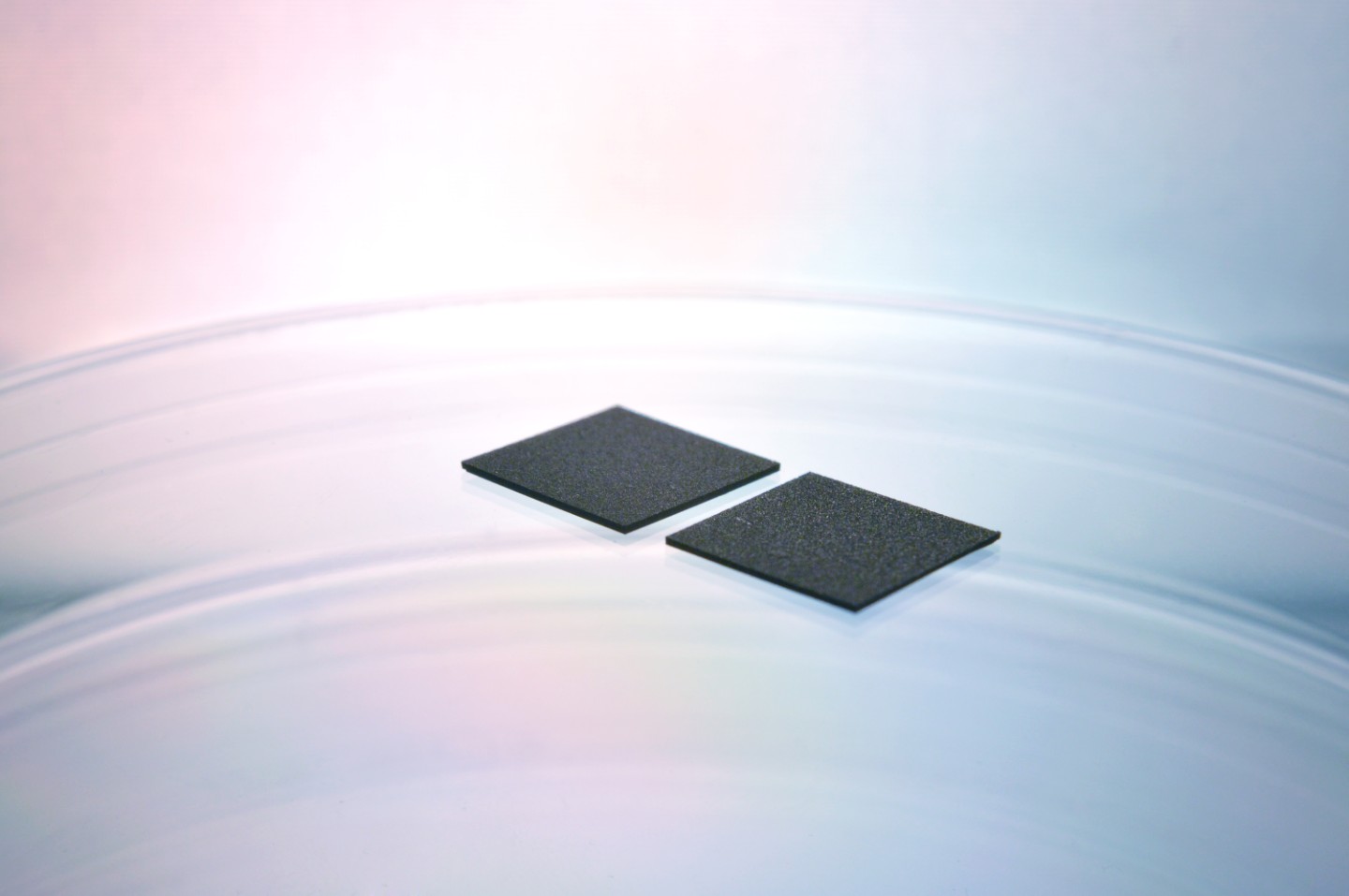
•          Free standing and semi free standing BDD foils

•          Flexible Parylene-C housed electrodes and

•          Micro fibers

© Fraunhofer USA CMW

Boron-Doped Diamond Fabrication Capabilities

Boron-doped diamond (BDD) fabrication capabilities range from diamond growth via post growth fabrication to assembly and material evaluation. BDD films can be applied on a variety of substrate materials and geometries. Post diamond growth capabilities include polishing, photolithography, etching, metallization and laser-cutting.

Diamond is grown on a variety of substrates including but not limited to certain metals (including expanded metal mesh), quartz, pyrex, silicon and polycrystalline diamond. With the application and product in mind, substrates are carefully evaluated and individually pre-treated for optimized diamond growth and resulting diamond materials. In-house clean room microfabrication processes allow for 4” diameter wafer processing including PVD (metallization) and PE-CVD (SiO2 and Si3N4) thin film deposition, photolithography and plasma etching.

Diamond lapping, polishing and laser cutting complement the Center's capabilities striving towards a one stop solutions provider for BDD electrode development and prototypes.

© Fraunhofer USA CMW
BDD prototypes
© Fraunhofer USA CMW
500um x 500um BDD windows on silicon substrate
© Fraunhofer USA CMW
Custom fabricated BDD on silicon electrodes

Microelectrode Array

BDD microelectrode arrays (MEA) further decrease the intrinsically low background current of BDD, yielding electrodes capable of ultra-sensitive analyte measurements. These MEAs can be fabricated on various substrates with custom designs including electrically isolated individually addressable microelectrodes.

With excellent steady state behavior obtained from fabricated MEAs, electrodes are produced for a variety of applications in electroanalytical chemistry. These applications include traditional cyclic voltammetric analyses, trace heavy metal determination and neurotransmitter sensing using fast-scan cyclic voltammetry, among others. BDD MEAs are fabricated to meet customer demands, whether that be housed as a traditional electrochemical rod-electrode or a microchip for small sample volumes.

© Fraunhofer USA CMW
Microelectrode Array
© Fraunhofer USA CMW
Hexagonal Microelectrode Array

Boron-Doped Diamond Optically Transparent Electrodes

Combining the advantage of rugged BDD material with optical transparency, BDD OTEs are excellent tools for spectroelectrochemical measurements. Applications range from the general study of redox chemistry (inorganic, organic, biological molecules) to spectroelectrochemical sensing where excellent sensitivity and selectivity can be obtained.

The BDD films are grown on quartz substrates and exhibit a wide range of optical transparency. Measurements can be made below 300 nm, a quality certain OTE materials can not achieve. The optical and electronic properties can be altered depending on experimental requirements; a more conductive film will be less optically transparent, while a more optically transparent film will be less conductive. Custom dimensions including microfabrication can be accommodated to fit a specific geometry.

© Fraunhofer USA CMW

Electrochemical Oxidation with Boron-Doped Diamond Electrodes

BDD electrodes have the proper combination of stability, ruggedness, and lifetime for use in electrochemical oxidation applications, including electrochemical advanced oxidation. These BDD electrodes have shown promise for use in many applications of water treatment. This includes per- and polyfluoroalkyl substance (PFAS) remediation as well as chemical oxygen demand (COD), total organic carbon (TOC), total ammonia nitrogen (TAN), and total nitrogen removal from contaminated water. Electrochemical oxidation processes with BDD electrodes can also work to reduce turbidity of wastewater samples. For all electrochemical oxidation applications, customization of BDD electrodes to fit your experimental needs is often required. More information about PFAS Remediation can be found here.

Additionally, if you are interested in investigating electrochemical oxidation using BDD electrodes for your water treatment application, we can test your water for you! COD, TOC, TN, and TAN measurements can be conducted in-house.

© Fraunhofer USA CMW

Disk Electrodes

© Fraunhofer USA CMW
Disk Electrodes

BDD disk electrodes offer superior electrochemical performance to other commercially available electrodes. Standard electrodes embed a 2mm polished BDD disk in a 6cm long x 6mm outer diameter PEEK housing. Custom orders with other chemical resistant housings, including PTFE, are possible.

With a lower capacitive background current and wider potential window to other competing electrode materials such as glassy carbon (GC), Fraunhofer USA CMW BDD disk electrodes can be used for electroanalytical measurements with ease. As seen above, many electrode materials including GC exhibit background voltammetric peaks that can potentially mask analyte current measurements. This is not observed on BDD disk electrodes as flat, featureless background currents are measured.

Diamond Plates

© Fraunhofer USA CMW
Diamond Plates

Free-standing BDD plates are available for a variety of applications and can be modified to fit specific experimental needs. BDD plates exhibit high electrical conductivity that is maintained at elevated temperatures, excellent mechanical and chemical rigidity, and long-lifetime. BDD plates are as-grown, unpolished, and about 350 μm thick. The material is typically offered in 10 mm x 10 mm geometries (picture shown), but smaller and larger geometries can be accommodated.