 Fraunhofer USA Center Midwest CMW
Cleanroom/Micro-processing
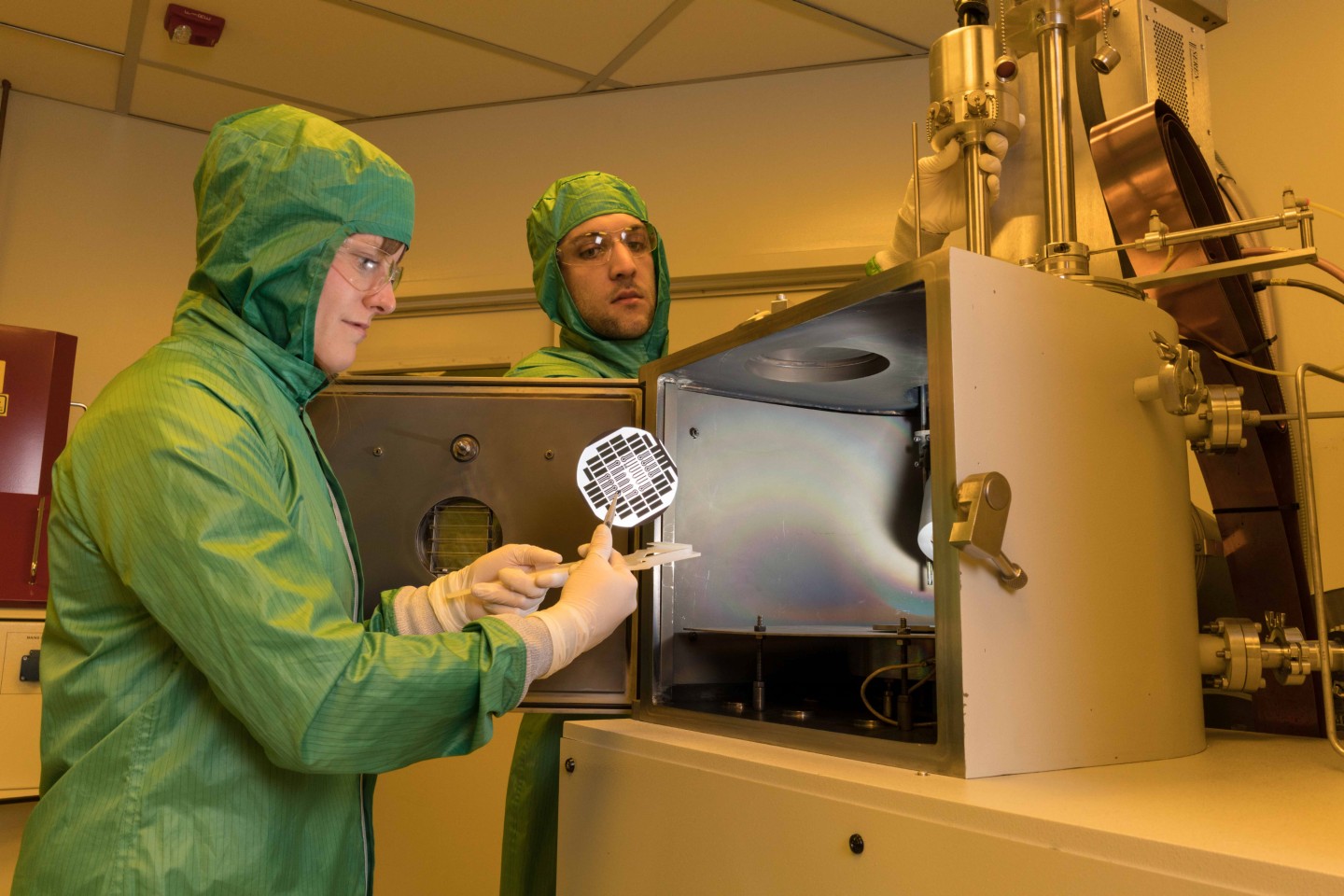
The center has access to semiconductor processing capabilities in a class 1000 cleanroom environment with an incorporated class 100 facility for photolithography.
Processing equipment includes traditional mask aligners and e-beam lithography for microstructure development. The mask aligner can be used for sub-µm structure on wafer sizes up to 4 inches. Processes are established for positive, negative and reversible photoresists. E-beam lithography equipment enables structuring with feature sizes down to 20 nm, however at a significantly larger exposure time and requires conductive substrates.
Metallization capabilities include a magnetron sputter/e-beam evaporation combination system with substrate heating and a thermal evaporator. Deposition of up to three metals at a time is possible. Metals include gold, platinum, titanium, molybdenum, chromium, nickel copper, and aluminum among others. Aluminum and copper are primarily used as protective metals for selective dry etching, while the others are mainly used for Ohmic and Schottky contact metallization.
Different plasma etchers using electron cyclotron resonance (ECR) and inductively coupled plasmas (ICP) are available for dry etching of material. Available gases for reactive ion etching are O2, SF6, CF4 and Ar. The systems are capable of processing 4-inch wafers.
A plasma-enhanced chemical vapor deposition (PECVD) system for the deposition of silicon dioxide using silane is available.
Furnaces are available for thermal oxidation (i.e. silicon to silicon oxide [SiO2]), diffusion doping (p-type and n-type) and for annealing in oxygen and inert atmospheres. Additionally, a vacuum annealing furnace is available.
A wet-chemical laboratory adds capabilities for etching of metals and back-etching of silicon.
We have access to an atomic layer deposition (ALD) system for deposition of SiO2. The system is located in a facility outside of a cleanroom environment.
Micro-processing is employed in the fabrication of BDD electrodes and SCD electronics.